
Quantum Materials
Quantum materials is a research field at the intersection of materials science, condensed matter physics, device engineering, and quantum information. Beyond traditional quantum materials such as unconventional superconductors and heavy fermion systems, the field has recently expanded to encompass topological quantum matter, two-dimensional materials and heterostructures, Floquet time crystals, as well as materials and devices designed for quantum computation with Majorana fermions.

Figure 1. Array of identical vertical nanowires grown by III-V Molecular Beam Epitaxy. Each nanowire is a few micrometers tall and has a diameter around 100 nm.
At Center for Quantum Devices we focus on hybrid materials, combining semiconducting, magnetic and superconducting elements, either in two-dimensional heterostructures or one-dimensional geometries based on nanowires (Fig. 1 shows an example of the latter). Materials are grown in-house by Molecular Beam Epitaxy (III-V MBE) and investigated structurally by e.g. Transmission Electron Microscopy. The MBE semiconductor growth is often combined with in-situ techniques for fabricating patterned nanostructures and new hybrid superconductors (Fig. 2). These materials are eventually implemented in devices for transport studies of topological systems, new types of superconducting qubits and coupled dots for quantum simulations.
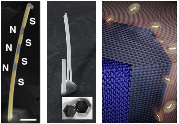
Figure 2. Nanowire with superconducting (S) and normal semiconducting (N) segments [1], a custom designed double nanowire with a shadowed superconducting coating at the top [2], and electron microscopy rendering of a semiconducting nanowire (blue) with facets coated epitaxially by a superconductor (red), inducing superconductivity in the semiconductor, symbolized here by the Cooper pairs of electrons [3].
QDev researchers pioneered the development of hybrid nanowires [4] that have been used in devices by numerous other research groups worldwide. More recently we have designed nanowire junctions, planar structures based on Selected Area Growth of semiconducting circuits with superconducting layers as well as materials with ferromagnetic insulators [5]. Some of the visions for future quantum materials are outlined in the Roadmap for Quantum Materials, co-authored by QDev staff [6]. Several materials and device concepts from QDev have been patented.
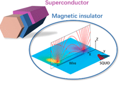
Figure 3. Semiconductor–ferromagnetic insulator–superconductor (InAs/EuS/Al) nanowire heterostructure [5].
[1] D. Carrad et al., Shadow Epitaxy for In Situ Growth of Generic Semiconductor/Superconductor Hybrids, Advanced Materials (2020)
[2] T. Kanne et al., Double nanowires for hybrid quantum devices, Advanced Functional Materials (2021)
[3] T. Kanne et al., Epitaxial Pb on InAs nanowires for quantum devices, Nature Nanotechnology (2021)
[4] P. Krogstrup et al., Epitaxy of semiconductor–superconductor nanowires, Nature Materials (2015)
[5] Y. Liu et al., Semiconductor–Ferromagnetic Insulator–Superconductor Nanowires: Stray Field and Exchange Field, Nano Letters (2020)
[6] F. Giustino et al., The 2021 Quantum Materials Roadmap, J. Phys. Materials (2021)