
Novel Devices
The nanoscale materials and experimental techniques used in quantum devices are useful also for other areas in physics and nanotechnology. One such example is the periodic array of nanowires developed originally for electronic devices. QDev research naturally leads to new types of devices and fabrication schemes. Researchers within the Center along with groups at the Nano-Science center and external collaborators investigate devices for advanced applications ranging from solar cells to biosensors.
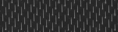
Array of vertical nanowires grown by III-V Molecular Beam Epitaxy. Each nanowire is a few micrometers tall and has a diameter around 100 nm (courtesy of M.H. Madsen).
Nanostructured materials are interesting for photovoltaic devices since the conversion efficiency can be increased by clever design of their geometry and the amount of active material can be minimized. For instance, efficient solar cells can be manufactured from gallium arsenide nanowires. We investigate photovoltaic devices based in individual standing nanowires that absorb visible light extremely efficiently. The wires have a built-in core-shell p-n junction and can be grown on inexpensive silicon substrates. This work is done in collaboration with EPFL, Switzerland [1].
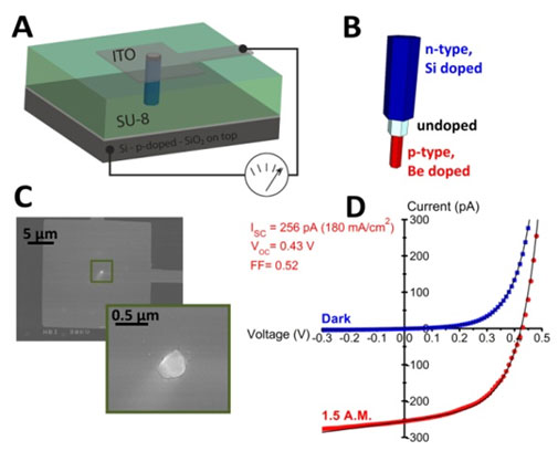
Single nanowire solar cell (A) based on a core-shell GaAs nanowire (B) on silicon with a transparent top-electrode (C). Exposed to a standard solar illumination (1.5 AM), the single wire generates a current of 0.25 nA (courtesy of P. Krogstrup).
1] P. Krogstrup et al., Absorption Boost in Single GaAs Nanowire Solar Cells on Silicon (submitted)
Highly uniform arrays of nanowires grown by Molecular Beam Epitaxy (MBE) are interfaced with living cells in collaboration with the Bionano-technology group of the Nano-Science Center [2]. The arrays can be used for probing of biological events locally in cells, either using fluorescent microscopy techniques or electro-active nanowires. Nanowires in field-effect transistor geometry are also employed as chemical and biological sensors, e.g. for detection of minute amounts of proteins in solution. These activities belong to the Bionanoelectronics workgroup of the larger Synthetic Biology program of University of Copenhagen https://synbio.ku.dk/
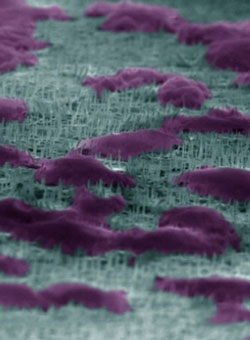
Human cells grown on vertical nanowires
(false color electron microscopy image, courtesy
of T. Berthing, Bionanotechnology group).
2] T. Berthing et al., Intact mammalian cell function
on semi-conductor nanowire arrays: new perspectives for cell-based bio-sensing, SMALL 7, 640
(2011).
Nanofabrication is also used to prepare devices for studies of electron transport in molecules. Novel devices for molecular electronics are manufactured by sandwiching self-assembled monolayers (SAM) of conducting molecules with graphene protection layers between planar metal source/drain electrodes. While the role of the molecules is to provide a given functionality to the device, the graphene acts as a protection layer, preventing the evaporated metal top-electrodes from penetrating the SAM in this vertical device geometry [4]. Various types of graphene are integrated in these devices, incl. chemically derived and grown graphene. This type of work is done jointly with the Nanochemistry group, Dept. of Chemistry, and in collaboration with groups at the Technical University of Denmark.
.
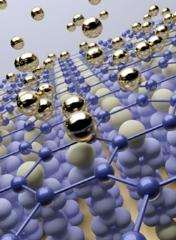
A graphene sheet on top of a layer of short conjugated molecules protecting it during deposition of a gold top-contact (courtesy of K. Nørgaard).
4] T. Li, J.R. Hauptmann et al., Solution Processed Ultrathin Chemically Derived Graphene Films as Soft Top Contacts for Solid-State Molecular Electronic Junctions, Advanced Materials 24,
1333 (2012).