Sjoerd Telkamp
ETH
Development of a Semiconductor-Superconductor Hybrid 2DEG with In-situ Nb and NbTi.
S. Telkamp1, T. Antonelli1,2 , C. Todt1, M.Hinderling2, M. Coraiola2, E. Cheah1, R. Schott1, F.
Křížek1,3, F. Nichele2, & W. Wegscheider1
1Advanced Semiconductor Quantum Materials Group, ETH Zurich, 8092 Zürich, Switzerland;
2IBM Research Europe, 8803 Rüschlikon, Switzerland3Institute of Physics, Czech Academy of Sciences, 162 00 Prague, Czech Republic
Křížek1,3, F. Nichele2, & W. Wegscheider1
1Advanced Semiconductor Quantum Materials Group, ETH Zurich, 8092 Zürich, Switzerland;
2IBM Research Europe, 8803 Rüschlikon, Switzerland3Institute of Physics, Czech Academy of Sciences, 162 00 Prague, Czech Republic
Semiconductor-superconductor hybrid structures ranging from quasi 1D-nanowires to 2D electron gases (2DEG) have recently emerged as a platform to study interaction between confined electronic states in the semiconductor and superconductivity [1][2]. Studying states that result from this coupling, such as Andreev Bound States (ABS), requires transparent interfaces between the semiconductor and superconductor. Most of the state of the art experiments rely on MBE-grown InAs combined with insitu deposited epitaxial Al films [3]. More recently, promising results were shown using other superconductors, e.g. Sn [4], Pb [5] or Nb [6], which offer a larger operating range in temperature and magnetic field. In this project, we have developed a new hybrid material combination based on Nb and NbTi as the superconductor. We implemented a novel method to deposit an in-situ Nb/NbTi thin film by magnetron sputtering on a shallow InAs 2DEG using a thin Al interlayer to avoid intermixing.
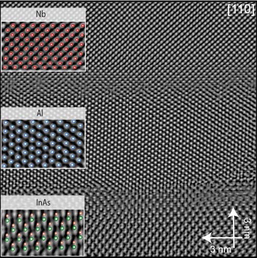
Guided by STEM analysis, we optimised the material stack to form highly crystalline interfaces obtaining a well-defined epitaxial relationship. Furthermore, transport measurements of Josephson junctions fabricated from this material show an induced gap of around 1.0 meV, only 2 times smaller than bulk Nb. Our results highlight the
crucial role played by the interface in determining the performance of hybrid systems and introduce a new methodology for maximizing the semiconductor-induced gap.

Electron Microscopy image showing the local epitaxy of the developed semiconductor-superconductor hybrid material.
References
[1] Lutchyn, R. M., Bakkers, E. P. A. M., Kouwenhoven, L. P., Krogstrup, P., Marcus, C. M., & Oreg, Y, Nature Reviews Materials, 3, 52–68 (2018).
[2] Frolov, S. M., Manfra, M. J., & Sau, J. D,Nature Physics, (2020).
[3] Chang, W., Albrecht, S. M., Jespersen, T. S., Kuemmeth, F., Krogstrup, P., Nygård, J., & Marcus, C. M., Nature Nanotechnology, 10, (2015).
[4] Pendharkar, M., Zhang, B., Wu, H., Zarassi, A., Zhang, P., Dempsey, C. P., Lee, J. S., Harrington, S. D., Badawy, G., Gazibegovic, S., Op het Veld, R. L. M., Rossi, M., Jung, J.,Chen, A. H., Verheijen, M. A., Hocevar, M., Bakkers, E. P. A. M., Palmstrøm, C. J., & Frolov, S. M., Science, 508–511, (2021).
[5] Kanne, T., Marnauza, M., Olsteins, D., Carrad, D. J., Sestoft, J. E., Bruijckere, J., Zeng, L.,Johnson, E., Olsson, E., Grove-Rasmussen, K., & Nygård, J. Nature Nanotechnology.(2021)
[6] Perla, P., Fonseka, H. A., Zellekens, P., Deacon, R., Han, Y., Kölzer, J., Mörstedt, T., Bennemann, B., Espiari, A., Ishibashi, K., Grützmacher, D., Sanchez, A. M., Lepsa, M. I., & Schäpers, T., Nanoscale Advances, 3, 1413–1421, (2021).
